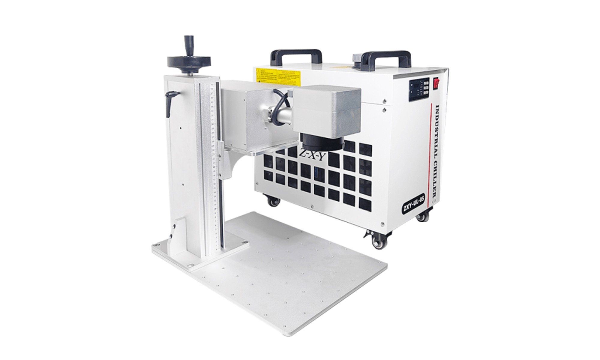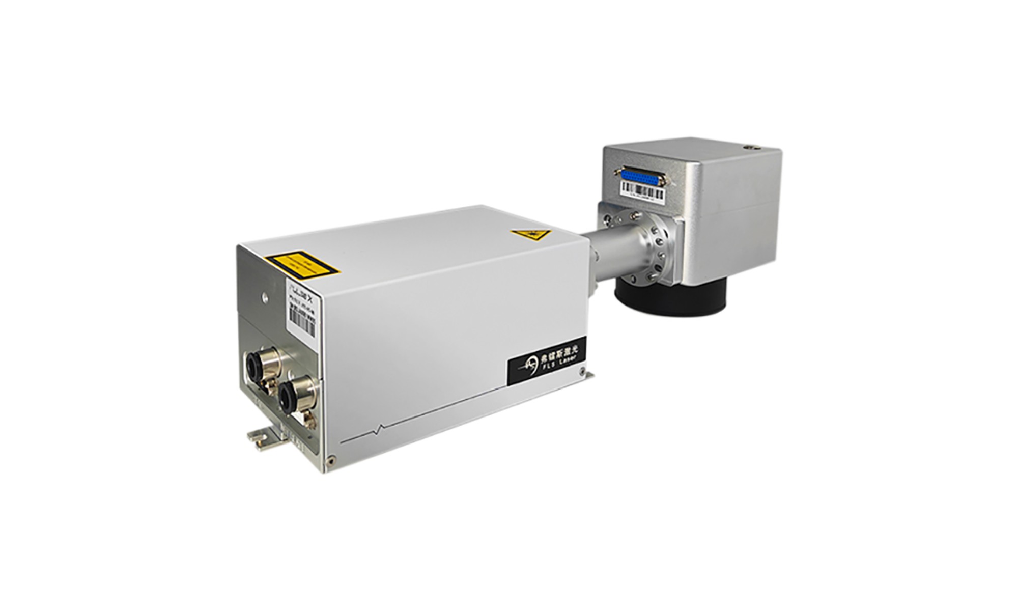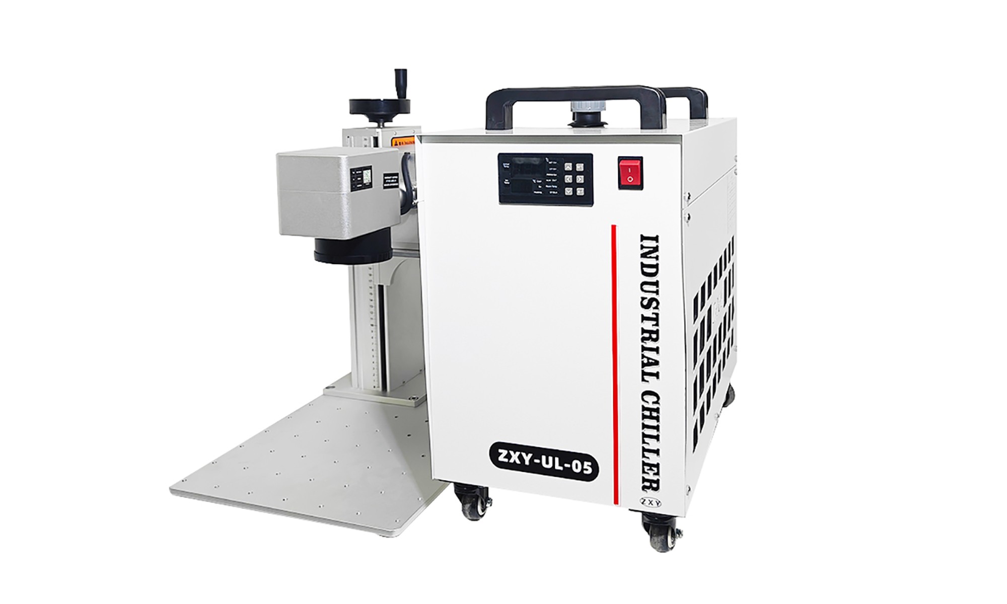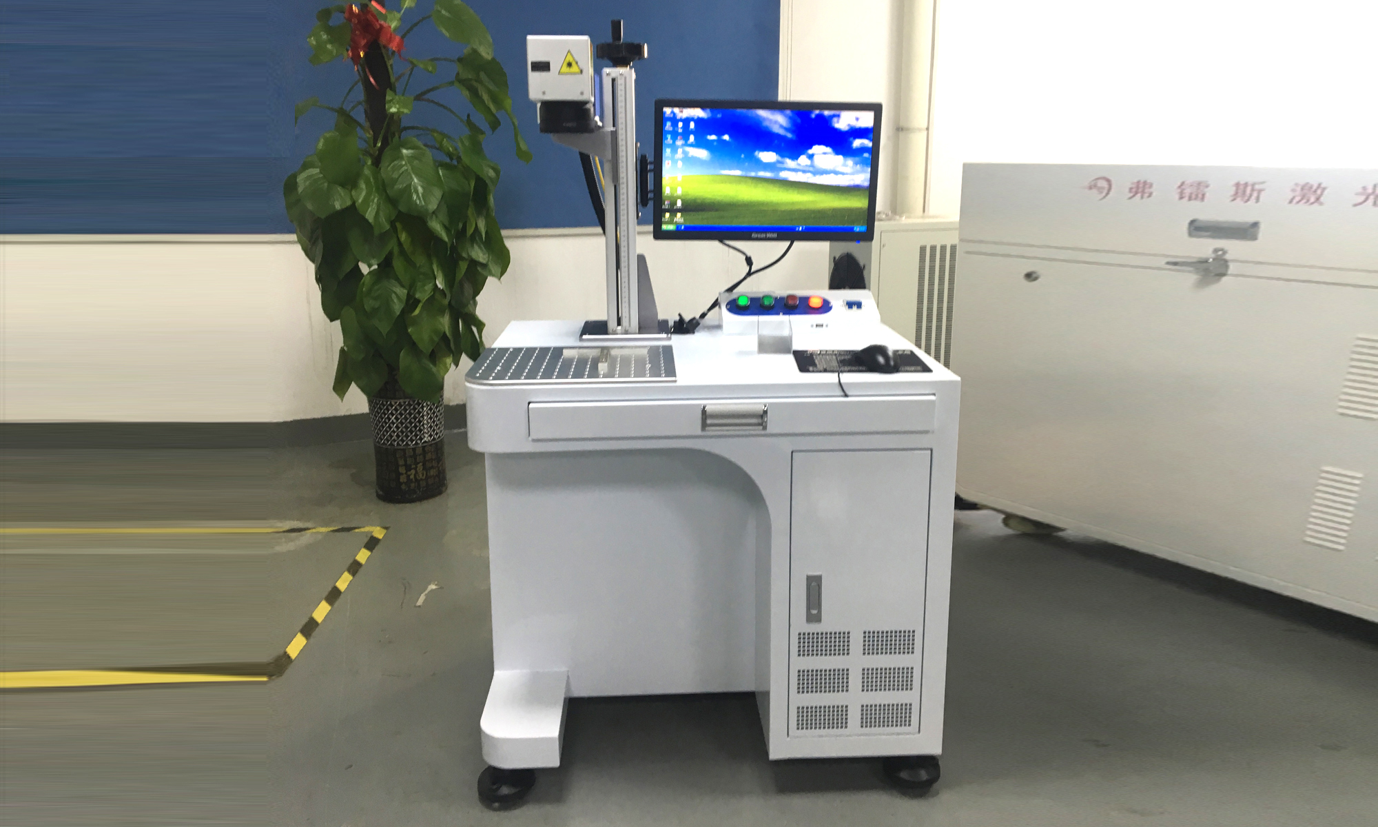
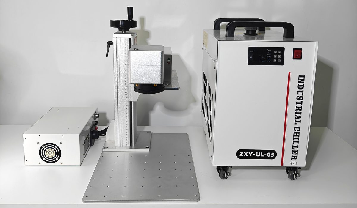
A semiconductor laser marking machine is a high-precision industrial cold-processing system purpose-built for the semiconductor and microelectronics manufacturing sector. It uses optimized 355nm ultraviolet or high-stability fiber laser sources to create ultra-fine, near-zero thermal-damage permanent marks on silicon wafers, crystal oscillators, lead frames, IC packages, PCBs and tiny microelectronic components. This semiconductor laser marking machine processes material through controlled photochemical ablation, not excessive heat melting. It is the most reliable marking solution for modern miniaturized semiconductor parts that cannot tolerate any surface deformation, circuit damage or micro-cracks.
Unlike general-purpose industrial laser markers that are designed for thick, large-format workpieces, a professional semiconductor laser marking machine is built for micron-level precision, 24/7 non-stop operation and full traceability requirements. In this guide, we break down everything you need to know about this system. We cover its core advantages, key semiconductor industry applications, critical specifications to compare, 2026 real pricing ranges and a practical 5-step selection checklist.
Why a Standard Industrial Laser Cannot Replace a Semiconductor Laser Marking Machine
Most manufacturing teams that first try to deploy a general-purpose laser marker on semiconductor production lines quickly run into hard performance limits. Standard industrial lasers often leave an obvious heat-affected zone. This can cause tiny thermal stress on the wafer surface, damage nearby micro circuits or even create invisible micro-cracks inside brittle semiconductor materials.
A professional semiconductor laser marking machine solves these problems from the core optical design level. Its laser beam is far more concentrated and precisely controlled. The heat-affected zone can be kept below 10μm, which will never affect the electrical performance or structural integrity of the surrounding tiny components.
For semiconductor production teams that have spent months fighting with fuzzy tiny 2D codes, cracked wafers and unqualified marking consistency, switching to a properly configured semiconductor laser marking machine is often the single upgrade that immediately eliminates 80% of their daily marking quality complaints.
Our semiconductor laser marking machine product line is built specifically for long-term high-precision semiconductor and microelectronics production.
Core Working Principles of a Semiconductor Laser Marking Machine
The full workflow of a semiconductor laser marking machine follows a highly controlled, ultra-low-heat processing sequence that never exposes delicate semiconductor parts to destructive thermal stress.
- High-Stability Laser Source Generates Optimized Wavelength Output
The dedicated laser source inside this semiconductor laser marking machine delivers extremely stable 355nm ultraviolet or 1064nm narrow-linewidth output. The power fluctuation rate is controlled below ±2%, which is far stricter than standard industrial laser requirements. - High-Speed Galvo Scanner Steers the Micron-Sized Beam
Two high-precision, low-vibration galvo mirrors steer the laser beam across the working field. They draw the exact vector marking path defined in your production marking file. - Telecentric F-Theta Lens Delivers Consistent Focus
A UV-optimized telecentric F-theta focusing lens compresses the laser energy into an extremely small spot, often smaller than 8μm. This ensures the spot size and marking precision stay perfectly consistent across the entire working field. - Photochemical Ablation Modifies Material Surface Gently
The high-energy laser photons break the molecular bonds on the top material layer directly. No excessive heat spreads to the surrounding area, so the semiconductor wafer or IC package will not experience any thermal deformation. - Ultra-Fine, High-Contrast Mark Forms Without Damage
The final result is a sharp, clear, permanent mark that can be as small as 0.03mm. It contains no burrs, no melting edges and no micro-cracks. The electrical performance and structural strength of the surrounding semiconductor part remain completely intact.
Every core optical component in a semiconductor laser marking machine must be strictly selected and optimized for semiconductor-grade processing. Using generic industrial optical parts will cause poor focus, unstable marking quality and hidden yield loss risks on high-value semiconductor production lines.
7 Core Advantages of a Semiconductor Laser Marking Machine
These unique performance benefits make a semiconductor laser marking machine irreplaceable in modern semiconductor manufacturing.
Micron-Level Ultra-Fine Marking Precision
A semiconductor laser marking machine can clearly mark characters and 2D codes smaller than 0.03mm. This level of precision is mandatory for modern miniaturized semiconductor components that leave almost no extra space for identification marks.
Near-Zero Heat-Affected Zone
The heat-affected zone generated by this system is typically smaller than 10μm. This means you can mark directly on ultra-thin wafers and tiny IC packages without causing warping, circuit damage or micro-cracks.
24/7 Ultra-Stable Long-Term Operation
Industrial-grade semiconductor laser marking machines are designed for non-stop production. Their power fluctuation rate stays below ±2% even after thousands of working hours. This level of consistency ensures zero unexpected quality drift on high-yield semiconductor production lines.
Full Traceability for Every Mark
The system automatically logs every marking operation, including serial number range, time stamp, operator ID, machine parameters and production batch. This full audit trail meets strict semiconductor industry traceability requirements.
Wide Material Compatibility for Semiconductor Parts
This machine performs reliably on silicon wafers, crystal oscillators, lead frames, IC packages, ceramic substrates, PCBs, FPC flexible boards and many special semiconductor packaging materials.
No Consumables, No Contamination Risk
The semiconductor laser marking process requires no ink, no solvents and no extra marking materials. It produces zero chemical waste and no residual contamination that could harm semiconductor part performance.
High-Speed Mass Production Capability
Modern semiconductor laser marking machines can process thousands of tiny components per minute. This easily keeps up with the high throughput rhythm of modern semiconductor packaging and testing production lines.
Key Industry Applications
A semiconductor laser marking machine is widely deployed across every major segment of the semiconductor and microelectronics manufacturing industry.
- Silicon Wafer Marking: Marking unique identification codes and alignment reference marks on bare silicon wafers before dicing.
- IC Package Marking: Printing part numbers, lot codes, traceability 2D codes and manufacturer logos on finished IC chips and packaging housings.
- Lead Frame Marking: High-speed continuous marking on metal lead frames during the semiconductor packaging process.
- Crystal Oscillator Marking: Ultra-fine marking on tiny crystal resonator components that cannot tolerate any thermal stress.
- PCB & FPC Marking: Marking identification codes and alignment marks on bare rigid PCBs and ultra-thin flexible FPC boards.
- Semiconductor Ceramic Substrate Marking: Creating high-contrast permanent marks on high-temperature ceramic packaging substrates.
- Micro-Sensor Component Marking: Marking serial numbers and calibration information on tiny MEMS micro-sensor parts.
- Semiconductor Packaging Tray Marking: Permanent, wear-resistant marking on reusable semiconductor material carrier trays.
If your semiconductor production line currently struggles with fuzzy tiny codes, hidden wafer cracks or unstable marking consistency, a professional semiconductor laser marking machine is almost always the technical upgrade that solves those problems permanently.
Critical Specifications to Evaluate
When comparing different semiconductor laser marking machines, these specifications will have the biggest real-world impact on your final production yield and long-term operational stability.
Laser Source Output Power Stability
The rated power fluctuation rate must be ≤ ±2%. This is the most fundamental requirement for consistent marking quality across thousands of semiconductor parts.
Minimum Focus Spot Size
For standard semiconductor marking applications, the spot size should be ≤ 10μm. For ultra-fine high-density 2D code marking, the spot size should be ≤ 8μm.
M² Beam Quality Value
The M² beam quality factor must be ≤ 1.2. Lower M² value means the laser beam is more concentrated, the spot is sharper, and marking quality is far more uniform across the entire working field.
Standard Working Field Size
Common industrial working fields are 110×110mm and 150×150mm. Larger working fields allow you to process more parts in one batch, but must maintain the same micron-level precision across the full area.
Galvo Scanner Repeat Position Accuracy
The galvo scanner must deliver a repeat position accuracy of ±1μm or better. This ensures every mark stays in exactly the same pre-defined position on every single part.
Vision Auto-Alignment Function
Integrated machine vision system automatically locates the part position, corrects placement offset and triggers marking. This eliminates all manual alignment errors completely.
Industrial Communication Protocol Support
The system must support standard industrial protocols including TCP/IP, OPC UA, Modbus and SQL database connection. This allows seamless integration with your existing semiconductor manufacturing execution system.
24/7 Continuous Working Rating
The machine must be rated for 24-hour non-stop continuous operation. It should not require frequent long downtime for cooling or maintenance during normal production.
2026 Real Industrial Price Ranges
A semiconductor laser marking machine is far more technically demanding than standard industrial laser markers. Its industrial pricing reflects the high-precision optical components, strict stability requirements and long-term reliability design. Below are realistic 2026 industrial price ranges for reference.
表格
| Configuration | Entry Semiconductor Grade | Mid-Range Industrial Semiconductor | High-End FAB Compliant System |
|---|---|---|---|
| 3W UV Semiconductor Marking System | 12,000–20,000 | 20,000–35,000 | 35,000–60,000+ |
| 5W UV Semiconductor Marking System | 18,000–28,000 | 28,000–45,000 | 45,000–75,000+ |
| High-Stability Fiber Semiconductor System | 15,000–25,000 | 25,000–40,000 | 40,000–65,000+ |
The biggest hidden cost of buying a low-cost non-semiconductor grade laser marker is not the initial purchase price. Unstable marking quality can cause hidden yield loss on high-value semiconductor parts. This loss can easily exceed the full cost of the machine in just a few months of production.
A properly configured semiconductor laser marking machine usually delivers full return on investment within 12 to 24 months, through improved yield, reduced rework and eliminated consumable cost.
5-Step Practical Selection Checklist
Follow this clear workflow to select the right semiconductor laser marking machine for your production line.
- List all your primary semiconductor workpiece materials — this immediately confirms which laser wavelength and power level is the correct choice.
- Define your minimum required mark size — if you need to mark 2D codes smaller than 0.1mm, you will need the highest precision optical configuration.
- Confirm your daily production throughput target — this tells you what marking speed and batch processing capacity you need to match your line rhythm.
- Send real sample parts for full marking test — never decide based only on spec sheets. Watch the actual marking result on your exact semiconductor parts.
- Verify MES integration and traceability functions — confirm the system can connect to your existing production management system and generate complete audit records.
Not sure which configuration fits your semiconductor parts best? Send us your material sample, and our semiconductor laser engineers will run a free full marking test and send you back high-resolution photos and video of the actual result.
Why Choose Shenzhen FLS Laser Semiconductor Laser Marking Systems
Shenzhen FLS Laser is a direct industrial laser equipment manufacturer with more than 12 years of high-precision laser R&D and manufacturing experience.
- All semiconductor laser marking machines use top-tier brand ultra-stabilized laser sources.
- Power fluctuation rate strictly controlled below ±2%, meeting semiconductor production stability requirements.
- Full CE, FDA and ISO certification, meeting global industrial semiconductor manufacturing standards.
- 2-year full machine warranty, lifetime technical support and free software updates.
- Free semiconductor sample marking service: send us your wafer or IC part, we mark it for free and send you back full test report.
- Customizable options including vision alignment systems, automatic loading/unloading stations and cleanroom compatible design.
- Full English operation videos, user manuals and remote online training are included with every machine.
Frequently Asked Questions
Q: Can a semiconductor laser marking machine mark on bare silicon wafers without cracking?
A: Yes. The ultra-low-heat processing mechanism creates almost zero thermal stress. It can mark on bare silicon wafers without causing cracks or material damage.
Q: What is the minimum 2D code size this system can clearly mark?
A: A high-quality semiconductor laser marking machine can clearly mark readable Data Matrix 2D codes as small as 0.03mm.
Q: Can this machine run 24 hours a day continuously?
A: Yes. Industrial-grade semiconductor laser marking machines are designed for 24/7 non-stop operation, with stable performance even after thousands of working hours.
Q: Can the system automatically connect to our semiconductor MES system?
A: Yes. The machine supports standard industrial communication protocols. It can seamlessly connect to most modern semiconductor manufacturing execution systems.
Q: Will laser marking affect the electrical performance of IC chips?
A: No. When configured with correct parameters, the process creates no thermal damage to surrounding circuits. It will not affect the electrical performance of IC chips.
Ready to upgrade your semiconductor marking quality and eliminate hidden yield loss? Contact Shenzhen FLS Laser today for a free semiconductor sample marking test and custom configuration recommendation.
Related Articles:How to Choose the Right Laser Marking System in Medical Devices