1. Product Overview
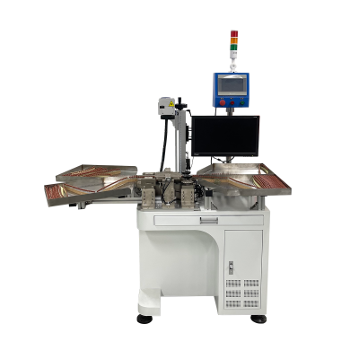
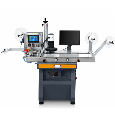
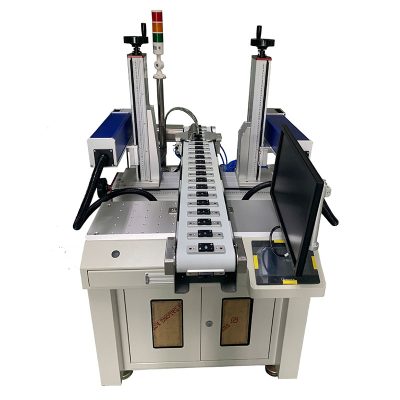
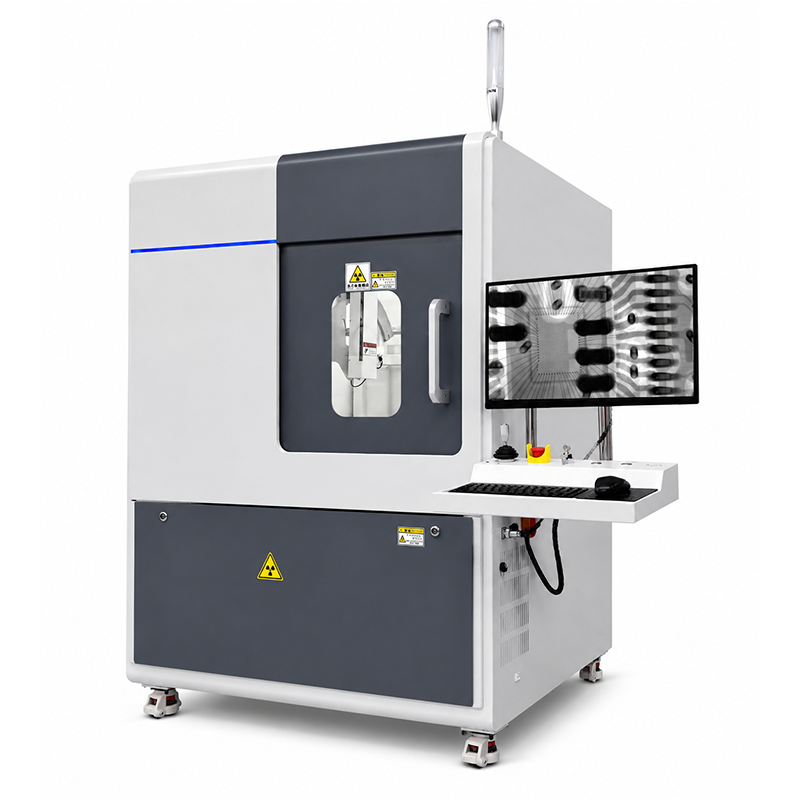
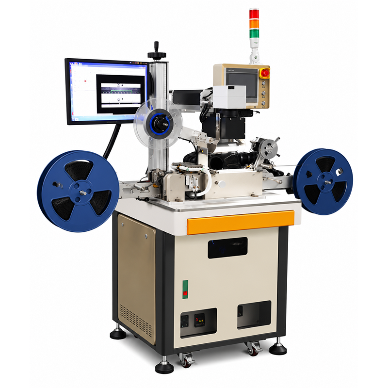
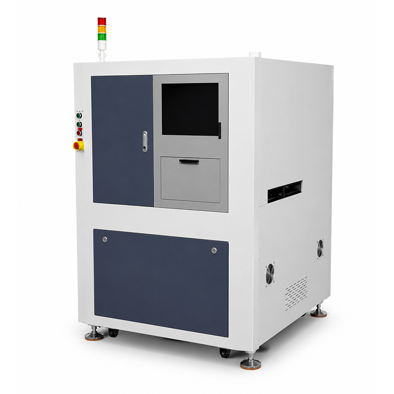
The Chip Laser Marking and Inspection Machine is an advanced semiconductor manufacturing solution integrating laser marking and vision inspection.
With a self-developed fiber laser source and self-developed laser marking inspection software, this Automatic Semiconductor Laser Marking and Vision Inspection System provides high stability, long lifetime and accurate quality control.
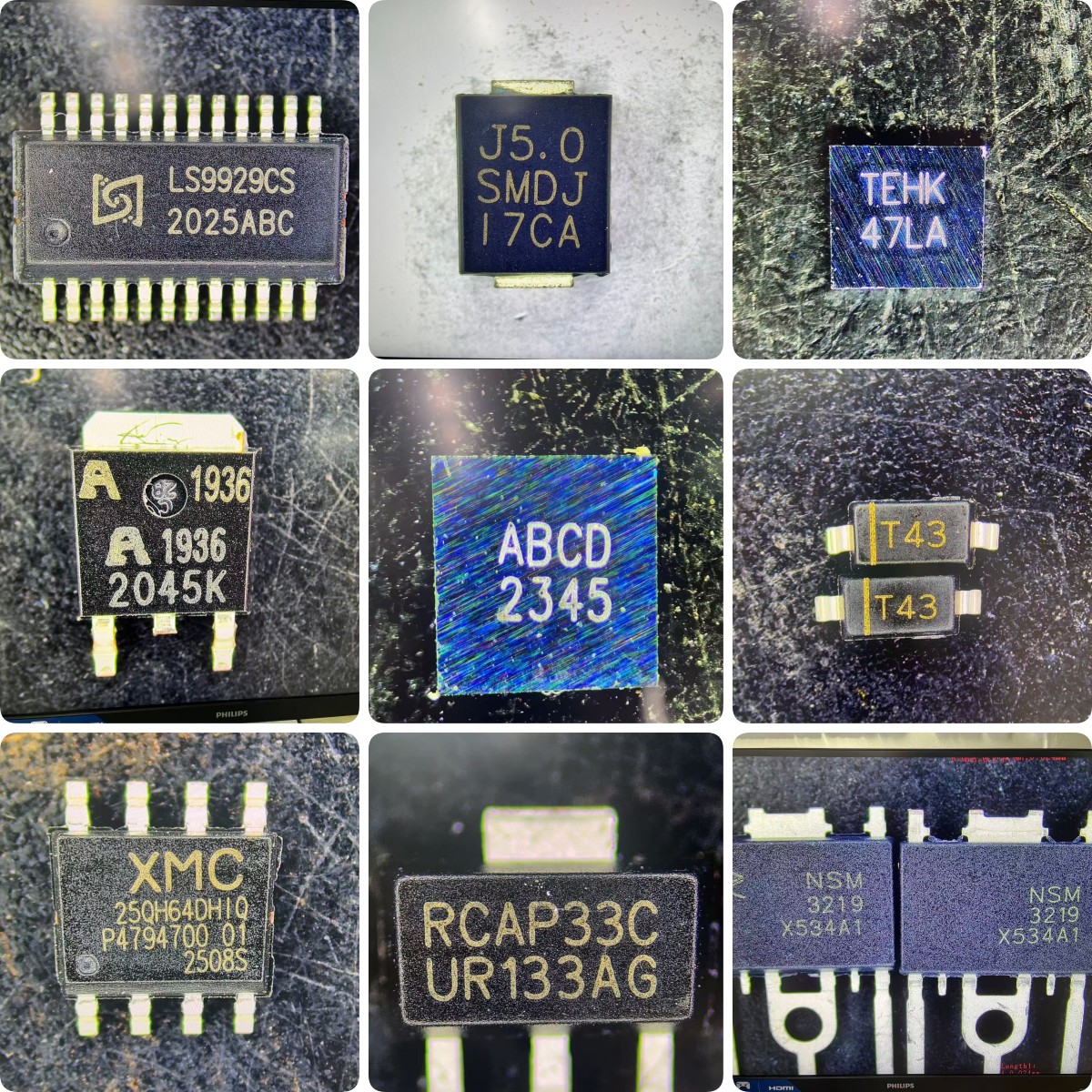
It is widely used for IC Laser Marking, Semiconductor Package Marking, QFN Laser Marking, DFN Laser Marking, SOP Package Marking, SOT Component Marking, MOSFET Marking, IGBT Marking and Power Device Traceability.
2. Product Advantages
• Integrated marking and inspection: Combines laser marking, OCR reading and defect detection.
• Self-developed laser source: Stable output, long lifetime and reliable performance.
• Self-developed software: Flexible control, inspection algorithms and customized functions.
• High precision marking: Suitable for semiconductor packages and micro electronic components.
• Vision positioning: Improves marking accuracy and product consistency.
• Automation ready: Supports Handler, Sorting Machine and MES integration.
• Permanent marking: No ink, no consumables and environmentally friendly.
3. Application Industries
Semiconductor Industry: IC packaging, semiconductor testing, chip identification and traceability.
Power Semiconductor Industry:
MOSFET, IGBT Module, Power Device and automotive semiconductor components.
Electronic Components:
Diodes, transistors, optocouplers, sensor chips and electronic modules.
4. Applicable Products
IC chips, QFN, DFN, SOP, SOT, TO220, TO252, TO263, MOSFET, IGBT modules, power semiconductor devices, optocouplers, sensor chips and electronic components.
5. Sample Test Video
6. Case